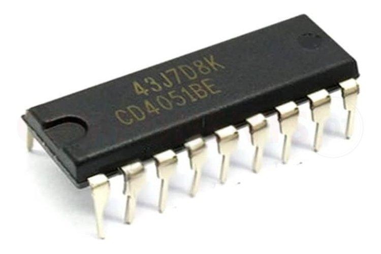
CD4051 8-Channel Analog Multiplexer/Demultiplexer with Logic-Level Conversion
The CD4051B is a digitally-controlled analog multiplexer/demultiplexer having a very low ON impedance and very low OFF leakage current. This is an 8-channel analog multiplexer/Demutiplexer and it has three digital control inputs. We can control the input/output using these control pins. It has an enable input (INH) that can be used to disable all the channels that is, disconnecting all the inputs from the output. The CD4051 can control analog signals with amplitudes up to 20 V peak-to-peak using digital signal amplitudes of 4.5 V to 20 V. The specific voltage levels for VDD, VSS, and VEE determine the range of analog signals that can be controlled by digital inputs. The CD4051 is commonly used in electronic circuits for signal routing and selection, such as in audio and video equipment, data acquisition systems, and instrumentation. This chip is available in different packages like 16-pin PDIP, CDIP, SOIC, SOP, and TSSOP
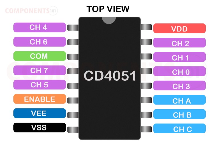
CD4051 Pinout Configuration
Here are the pinout details for CD4051.
| PIN NO | PIN NAME | DESCRIPTION |
| 1 | CH 4 IN/OUT | Channel 4 in/out |
| 2 | CH 6 IN/OUT | Channel 6 in/out |
| 3 | COM OUT/IN | Common out/in |
| 4 | CH 7 IN/OUT | Channel 7 in/out |
| 5 | CH 5 IN/OUT | Channel 5 in/out |
| 6 | INH | Disables all channels. |
| 7 | VEE | Negative power input |
| 8 | VSS | Ground |
| 9 | C | Channel select C. |
| 10 | B | Channel select B. |
| 11 | A | Channel select A. |
| 12 | CH 3 IN/OUT | Channel 3 in/out |
| 13 | CH 0 IN/OUT | Channel 0 in/out |
| 14 | CH 1 IN/OUT | Channel 1 in/out |
| 15 | CH 2 IN/OUT | Channel 2 in/out |
| 16 | VDD | Positive power input |
Manufacturers of CD4051:
The CD4051 is originally manufactured by Texas Instruments. However, several other manufacturers also produce compatible versions of this IC. Some of the manufacturers are ON Semiconductor, NXP Semiconductor and Analog Devices.
CD4051 Equivalents
If you are looking for an equivalent or replacement for CD4051 you can use the CD4052 and CD4053 from the same family. Keep in mind that, the CD4051 is a single eight-way multiplexer, the CD4052 has two four-way multiplexers, while the CD4053 has three two-way switches.
CD4051 Alternatives
If you are looking for an alternative for CD4051 you can look at the other IC from these.
74HCT4851D, MC14051B, ADG408
Note: Complete technical details can be found in the CD4051 datasheet at this page’s end.
Features of CD4051 Multiplexer/Demultiplexer IC
CD4051 CMOS Single 8-Channel Analog Multiplexer has the following key features:
- Wide range of digital and analog signal levels: – Digital: 3 V to 20 V –Analog: ≤ 20 VP-P
- Low ON resistance, 125 Ω (typical) over 15 VP-P signal input range for VDD – VEE = 18 V
- High OFF resistance, channel leakage of ±100 pA (typical) at VDD – VEE = 18 V
- Logic-level conversion for digital addressing signals of 3 V to 20 V
- 5 V, 10 V, and 15 V parametric ratings
- 100% tested for quiescent current at 20 V.
- The maximum input current of 1 µA at 18 V over the full package temperature range, 100 nA at 18 V and 25°C
- Available in different packages
How to use CD4051 IC in a Circuit?
The following image shows the typical CD4051 circuit diagram
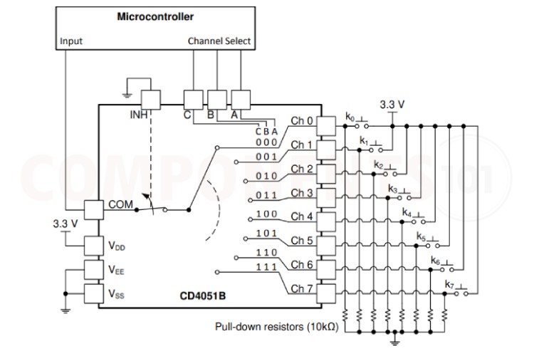
One application of the CD4051B is to use it in conjunction with a microcontroller to poll a keypad. The above image shows the basic schematic for such a polling system. The microcontroller uses the channel-select pins to cycle through the different channels while reading the input to see if a user is pressing any of the keys. This application is a very robust setup, allowing for multiple simultaneous key presses with very little power consumption. This setup also uses very few pins on the microcontroller. The downside of polling is that the microcontroller must continually scan the keys for a press and can do little else during this process.
CD4051 Not Working?
If you have just used the CD4051 multiplexer IC for the first time and if you are not able to get it working, check out the commonly faced problems below. If your question is not here, you can leave it in the comment section below
- The circuit’s performance is not stable. There is a lot of noise introduced to the line: Ensure that the power supply to the CD4051 is stable and within the specified voltage range. Each VCC terminal should have a good bypass capacitor to prevent power disturbance. For devices with a single supply, a 0.1-μF bypass capacitor is recommended. If there are multiple pins labeled VCC, then a 0.01-μF or 0.022-μF capacitor is recommended for each VCC because the VCC pins will be tied together internally. For devices with dual supply pins operating at different voltages, for example, VCC and VDD, a 0.1-µF bypass capacitor is recommended for each supply pin. It is acceptable to parallel multiple bypass capacitors to reject different frequencies of noise. 0.1-μF and 1-μF capacitors are commonly used in parallel. The bypass capacitor should be installed as close to the power terminal as possible for best results.
- The signals get clipped at a certain level: Inputs should not be pushed more than 0.5 V above VDD or below VEE. For input voltage level specifications for control inputs, see VIH and VIL in Electrical Characteristics.
- There is no current limit provided with CD4051: The CD4051 does not have internal current drive circuitry and thus cannot sink or source current. Any current will be passed through the device.
Design Tips for CD4051
1. How to minimize noise while using CD4051?
Use bypass capacitors (typically 0.1 μF) between VDD and VSS and between VEE and VSS to stabilize the power supply and minimize noise.
2. Does the working of the circuit depend on the temperature?
The CD4051's performance can vary with temperature, so operate it within the specified temperature range for best results.
3. What are the design considerations when designing a PCB using CD4051?
Reflections and matching are closely related to loop antenna theory but different enough to warrant their own discussion. When a PCB trace turns a corner at a 90° angle, a reflection can occur. This reflection is primarily due to the change in the width of the trace. At the apex of the turn, the trace width is increased to 1.414 times its width. This upsets the transmission line characteristics, especially the distributed capacitance and self–inductance of the trace — resulting in the reflection. It is a given that not all PCB traces can be straight, and so they will have to turn corners. The below image shows progressively better techniques for rounding corners. Only the last example maintains constant trace width and minimizes reflections.

Applications of CD4051
- Analog and digital multiplexing and demultiplexing
- Analog to digital and digital to analog conversion
- Signal gating.
- Factory automation
- Televisions
- Appliances
- Consumer audio
- Programmable logic circuits
- Sensors
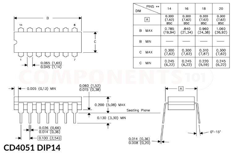
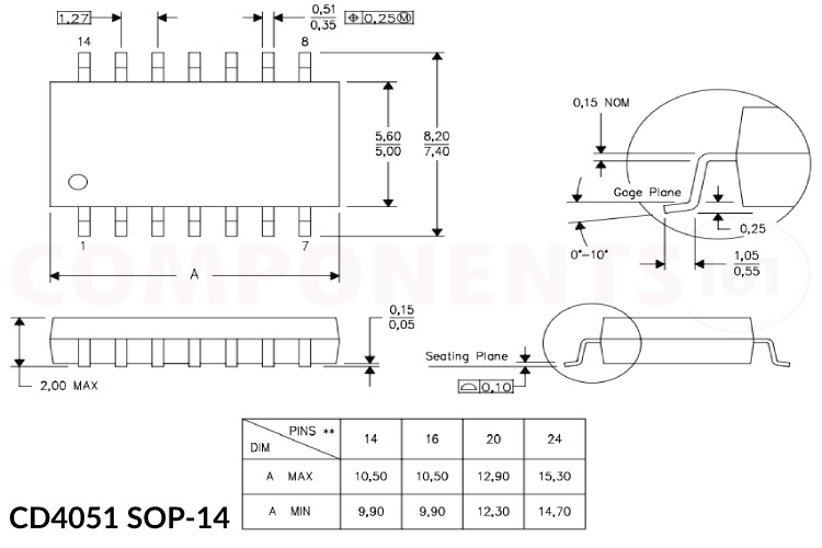
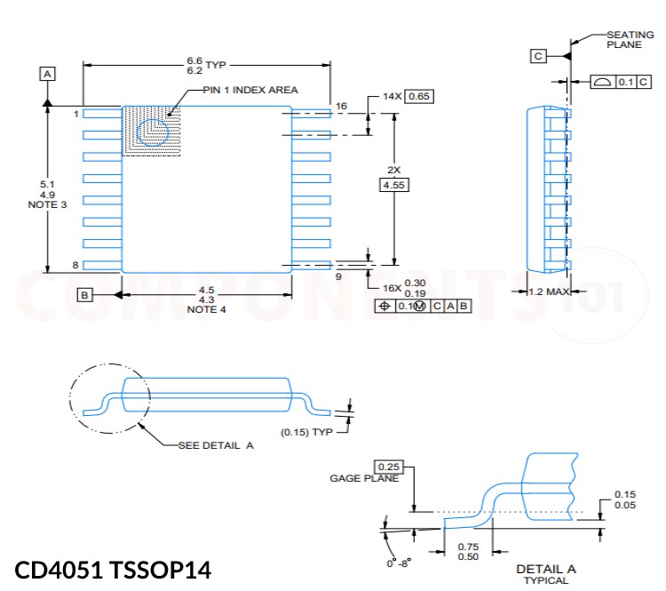
2D Model and Dimensions of CD4051
Here you can find the mechanical drawings of CD4051 along with its dimensions. The dimensions can be used to create custom footprints of the module and be used for PCB or CAD modeling.