

Capable of supporting up to 32 GT/s without altering design
Popular MOSFETs frequently used in Power Electronics Designs

MOSFET is one of the important components in Power Electronics and we have covered many MOSFETs with their Pin diagram, datasheet, features and how to use them in the circuit. Selecting a MOSFET for your project might be a daunting and time-consuming task as you have to go through the specification of each MOSFET. So here we decide to make a consolidated list of popular MOSFETs which can help in selecting the right MOSFET for your application.
So, if you are building some power electronics circuit and thinking about how to choose the right MOSFET for your specific application, here is a list of popular through-hole and surface mounted MOSFETs which you can find in your local or on online store.
BS170
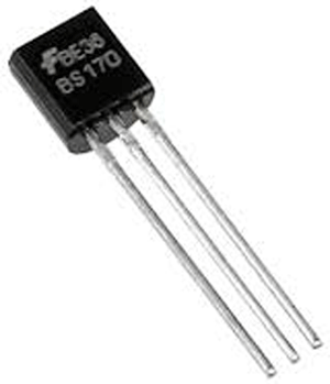
The BS170 is a most common N-channel enhancement mode MOSFET which is used by many electronic designers and hobbyists; it comes in a TO-92 package and performs best with low voltage low current applications.
Some basic features of BS170 MOSFET make it suitable for certain applications for example:
- It has a low threshold voltage of 2.1V which means it can be driven by a 3.3V logic level Microcontroller such as an Arduino.
- It has a low input capacitance of 22pF which makes it suitable for basic high-frequency switching drivers.
- Low on-resistance of 2.5 Ω improves the efficiency of this MOSFET for applications such as high power LED driver.
- It has very fast switching speed of 7ns, which means it can be used as a bidirectional logic-level converter for SPI, I2C & UART.
- It can be used as a low noise preamplifier, with a voltage amplifier configuration.
Most Important Parameters:
|
Rating |
Symbol |
Value |
Unit |
|
Drain−Source Voltage |
VDS |
60 |
Vdc |
|
Gate−Source Voltage − Continuous −Non−repetitive (tp ≤ 50 s) |
VGS VGSM |
±20 ±40 |
Vdc Vpk |
|
Drain−Source On-Resistance (VGS = 10 Vdc,ID = 200 mAdc) |
RDS(on) |
1.8 |
Ω |
|
Drain Current (Note) |
ID |
0.5 |
Adc |
|
Total Device Dissipation @ TA = 25°C |
PD |
350 |
mW |
|
Drain−Source Breakdown Voltage (VGS = 0, ID = 100 mAdc) |
V(BR)DSS |
90 |
Vdc |
|
Total Gate Charge (VDS = 30 V, ID = 0.5 A, VGS = 20) |
Qg (Max) |
2.4
|
nC |
|
Gate Threshold Voltage (VDS = VGS, ID = 1.0 mAdc) |
VGS(Th) |
2.0 |
Vdc |
|
Operating and Storage Junction Temperature Range |
TJ, Tstg |
−55 to +150 |
°C |
Part Number: BS170
Datasheet Link: BS170 MOSFET Datasheet link
Similar Products: BS170F
BS250
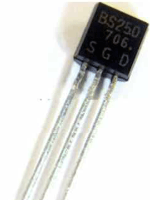
BS250 is a P-channel enhancement mode MOSFET in a TO-92 package, and it is designed to work with low voltage and low current applications. Listed below are some basic features of BS250 MOSFET which make it suitable for certain applications:
- It has a low threshold voltage of -1.9V which means it can be driven by a 1.8V logic level Microcontrollers.
- Since it is a P-channel MOSFET it can be used for high side switching applications
- Due to low on-resistance, it can drive up to .18A of a load.
- The fast switching speed of only 16 nS and the low input capacitance of only 15pF make it a suitable choice for many switching applications.
- It can be used as a driver for Relays, Solenoids, Lamps, Displays, Memories, Power Transistors, and Motors.
Most Important Parameters
|
Rating |
Symbol |
Value |
Unit |
|
Drain−Source Voltage |
VDS |
−45 |
Vdc |
|
Gate−Source Voltage − Continuous |
VGS |
± 25 |
Vdc |
|
Drain−Source On-Resistance (VGS = -10 Vdc,ID = -0.2 Adc) |
RDS(on) |
14 |
Ω |
|
Drain Current - Continuous - Pulsed |
ID IDM |
−0.18 2.2 |
Adc |
|
Total Device Dissipation @ TA = 25°C |
PD |
0.83 |
W |
|
Drain−Source Breakdown Voltage (VGS = 0, ID = 21 mA ) |
V(BR)DSS |
−45 |
Vdc |
|
Total Gate Charge |
Qg (Max.) |
1.8
|
nC |
|
Gate Threshold Voltage (VDS = VGS, ID = - 250 μA) |
VGS(Th) |
−1 to −3.5 |
Vdc |
|
Operating and Storage Junction Temperature Range |
TJ, Tstg |
−55 to +150 |
°C |
Part Number: BS250
Datasheet Link: Click here to open the datasheet
Similar Products: BSP254A, TP0610KL
Note: This is a common product can be found in a local store and its switching time is essentially independent of operating temperature.
BSS138
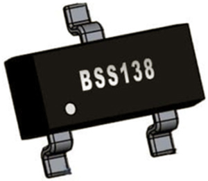
The BSS138 is the most common N-channel enhancement MOSFET produced using ON Semiconductor’s proprietary based on high cell density and DMOS technology, which is used by many electronic production firms, designers and hobbyist. It comes in a SOT-23 package and performs best with low voltage low current applications.
Some basic features of BSS138 MOSFET make it suitable for certain applications like:
- It has a very low Gate Threshold Voltage of 1.5V which means it can be driven by a 1.8V logic-level Microcontroller.
- It has a low input capacitance of 27pF@1MHz which makes it a suitable choice for basic high-frequency switching drivers.
- Low on-resistance of 3.5Ω and on-state drain current of 200mA makes it suitable for LED, Motor or Relay driver applications.
- It has a very fast switching speed of 20 nS which makes it a perfect choice as Bidirectional Logic-Level Converter.
Most Important Parameters
|
Rating |
Symbol |
Value |
Unit |
|
Drain−Source Voltage |
VDS |
50 |
Vdc |
|
Gate−Source Voltage − Continuous −Non−repetitive (tp ≤ 50 s) |
VGS VGSM |
±20 ±40 |
Vdc Vpk |
|
Drain−Source On-Resistance (VGS = 10 Vdc,ID = 200 mAdc) |
RDS(on) |
3.5 |
Ω |
|
Drain Current - Continuous - Pulsed |
ID |
.22 .88 |
Adc |
|
Total Device Dissipation @ TA = 25°C |
PD |
360 |
mW |
|
Drain−Source Breakdown Voltage (VGS = 0, ID = 100 mAdc) |
V(BR)DSS |
50 |
Vdc |
|
Total Gate Charge |
Qg (Max.) |
2.4 |
nC |
|
Gate Threshold Voltage (VDS = VGS, ID = 1.0 mAdc) |
VGS(Th) |
1.5 |
Vdc |
|
Operating and Storage Junction Temperature Range |
TJ, Tstg |
−55 to +150 |
°C |
Part Number: BSS138
Datasheet Link: Click here to open the datasheet
Similar Products: BSS123, BSS126H6327XTSA2
Note: This is a common product and can be found in a local store. Also, remember to design the PCB properly using this as improper PCB design can lead to thermal issues.
IRF540
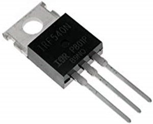
The IRF540 is another most common N-channel enhancement MOSFET which is used by many electronic designers and hobbyists. It comes in a TO-220AB package, so it is preferred for all commercial-industrial applications and performs best with low voltage high current applications. Low thermal resistance and low package cost of the TO-220AB makes it very popular in the industry. Some basic features and applications are listed below
- It has a low threshold voltage of 2.1V which means it can be driven by a 3.3V logic level Microcontroller such as an Arduino or PIC Microcontroller.
- It has a very low on-resistance of only 77 mΩ which makes it suitable for driving a heavy load.
- It is used in many switching applications due to fast switching speed and low input capacitance.
- Low on-resistance and low input gate capacitance make it suitable for parallel operations.
- Dynamic dv/dt prevents false switching, oscillation or permanent damage of a MOSFET.
Most Important Parameters
|
Rating |
Symbol |
Value |
Unit |
|
Drain−Source Voltage |
VDS |
100 |
Vdc |
|
Gate−Source Voltage − Continuous |
VGS |
± 20 |
Vdc |
|
Drain−Source On-Resistance (VGS = 10 Vdc,ID = 17 Adc) |
RDS(on) |
0.077 |
Ω |
|
Drain Current - Continuous - Pulsed |
ID IDM |
28 110 |
Adc |
|
Total Device Dissipation @ TA = 25°C |
PD |
150 |
W |
|
Drain−Source Breakdown Voltage (VGS = 0, ID = 250 μA) |
V(BR)DSS |
100 |
Vdc |
|
Total Gate Charge |
Qg (Max.) |
72 |
nC |
|
Gate Threshold Voltage (VDS = VGS, ID = 250 μA) |
VGS(Th) |
4 |
Vdc |
|
Operating and Storage Junction Temperature Range |
TJ, Tstg |
- 55 to + 175 |
°C |
Part Number: IRF540NPBF
Datasheet Link: Click here to open the datasheet
Similar Products: IRF520, IRF530, IRF640, IRF840
Note: This is a common product and can be found in a local electronics parts store.
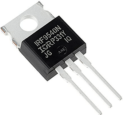
IRF9540
The IRF9540 is the most common P-channel enhancement mode silicon gate MOSFET which is used by many electronics designers and hobbyists. It comes in a TO-220 package, so it’s a perfect choice for all kinds of commercial-industrial applications, and it performs best with low voltage high current applications.
Some basic features and applications of IRF9540 MOSFET are listed below:
- Dynamic dv/dt prevents false switching, oscillation, or permanent damage to a MOSFET.
- It has a very low on-resistance of 0.2 Ω which improves the overall efficiency of the system.
- Since it is a P-channel MOSFET it can be used for high side switching applications
- This MOSFET is a perfect choice for inverter applications.
- Due to its wide operating temperature and low cost of it is widely accepted throughout the industry.
Most Important Parameters
|
Rating |
Symbol |
Value |
Unit |
|
Drain−Source Voltage |
VDS |
-100 |
Vdc |
|
Gate−Source Voltage − Continuous |
VGS |
± 20 |
Vdc |
|
Drain−Source On-Resistance (VGS = -10 Vdc,ID = -11 Adc) |
RDS(on) |
.20 |
Ω |
|
Drain Current - Continuous - Pulsed |
ID IDM |
- 19 - 72 |
Adc |
|
Total Device Dissipation @ TA = 25°C |
PD |
150 |
W |
|
Drain−Source Breakdown Voltage (VGS = 0, ID = - 250 μA ) |
V(BR)DSS |
-100 |
Vdc |
|
Total Gate Charge |
Qg (Max.) |
61 |
nC |
|
Gate Threshold Voltage (VDS = VGS, ID = - 250 μA ) |
VGS(Th) |
-4.0 |
Vdc |
|
Operating and Storage Junction Temperature Range |
TJ, Tstg |
- 55 to + 175 |
°C |
Part Number: IRF9540
Datasheet Link: Click here to open the datasheet
Similar Products: IRF9530NPBF, IRF9630PBF
Note: This is a common product and can be found in a local electronics parts store.
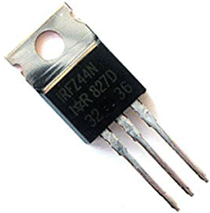
IRFZ44NPbF
The IRFZ44NPbF is another most common N-channel enhancement mode MOSFET designed with International Rectifier Advanced HEXFET® technology, and it is used by many electronic designers and hobbyists, due to its extremely low on-resistance. It comes in a TO-220 package, which is universally preferred for all commercial-industrial applications, so it performs best with low voltage low current applications.
Some basic features of IRFZ44NPbF MOSFET make it suitable for certain applications which are listed below:
- Dynamic dv/dt prevents false switching, oscillation or permanent damage to the MOSFET.
- It has a very low on-resistance of 17.5mΩ which maximizes the efficiency of the system.
- General-purpose applications like a motor driver, inverter, switching power supplies, DC-DC converters can be made from this MOSFET.
Most Important Parameters
|
Rating |
Symbol |
Value |
Unit |
|
Drain−Source Voltage |
VDS |
60 |
Vdc |
|
Gate−Source Voltage − Continuous |
VGS |
± 20 |
Vdc |
|
Drain−Source On-Resistance (VGS = -10 Vdc,ID = -11 Adc) |
RDS(on) |
0.028 |
Ω |
|
Drain Current - Continuous - Pulsed |
ID IDM |
50 200 |
Adc |
|
Total Device Dissipation @ TA = 25°C |
PD |
150 |
W |
|
Drain−Source Breakdown Voltage (VGS = 0, ID = - 250 μA ) |
V(BR)DSS |
60 |
Vdc |
|
Total Gate Charge |
Qg (Max.) |
67 |
nC |
|
Gate Threshold Voltage (VDS = VGS, ID = - 250 μA ) |
VGS(Th) |
4.0 |
Vdc |
|
Operating and Storage Junction Temperature Range |
TJ, Tstg |
- 55 to + 175 |
°C |
Part Number: IRFZ44NPbF
Datasheet Link: Click here to open the datasheet
Similar Products: IRFZ20, IRFZ24NPBF, IRFZ34PBF, IRFZ44NPBF
Note: This is a common product and can be found in a local electronics parts store. Also, note that its Continuous Drain Current (ID) is limited by the Package.
IRLZ44N
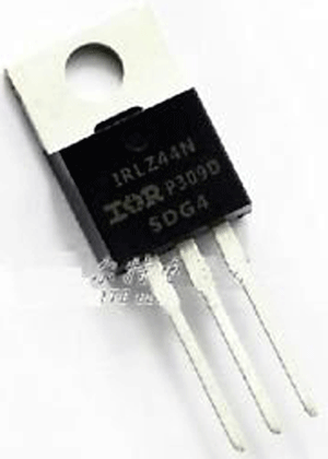
The IRLZ44N is another most common N-channel enhancement mode MOSFET, designed with International Rectifier Fifth Generation Advanced HEXFET® technology. It is used by many electronic designers because it comes in a TO-220 package, which is universally preferred for all commercial-industrial applications and it performs best with low voltage low current applications.
Some basic features of IRLZ44N MOSFET make it suitable for certain applications which are listed below:
- It is a logic level MOSFET which means it can be driven by many different types of Microcontroller.
- Low on-resistance of this MOSFET makes it suitable for many high-current drive applications.
- It supports many High current MOSFET gate driver ICs due to low Input capacitance of the only 3.3nF.
- Dynamic dv/dt prevents false switching, oscillation or permanent damage of a MOSFET.
- This MOSFET can be used for many general purpose applications like H-Bridge motor driver, power MOSFET gate driver and many more.
Most Important Parameters
|
Rating |
Symbol |
Value |
Unit |
|
Drain−Source Voltage |
VDS |
60 |
Vdc |
|
Gate−Source Voltage − Continuous |
VGS |
± 10 |
Vdc |
|
Drain−Source On-Resistance (VGS = -10 Vdc,ID = -11 Adc) |
RDS(on) |
0.028 |
Ω |
|
Drain Current - Continuous - Pulsed |
ID IDM |
50 200 |
Adc |
|
Total Device Dissipation @ TA = 25°C |
PD |
150 |
W |
|
Drain−Source Breakdown Voltage (VGS = 0, ID = - 250 μA ) |
V(BR)DSS |
60 |
Vdc |
|
Total Gate Charge |
Qg (Max.) |
66 |
nC |
|
Gate Threshold Voltage (VDS = VGS, ID = - 250 μA) |
VGS(Th) |
2.0 |
Vdc |
|
Operating and Storage Junction Temperature Range |
TJ, Tstg |
- 55 to + 175 |
°C |
Part Number: IRLZ44N
Datasheet Link: Click here to open the datasheet
Similar Products: IRLZ34PBF, IRLZ14PBF
Note: This is a common product and can be found in a local electronics parts store. It is current limited by the package so consider the datasheet while selecting the package.
SSM6N7002KFU, LF
The SSM6N7002KFU, LF is an uncommon N-channel enhancement MOSFET and comes in a US6 package, so it can be used in some very compact products and applications. Very low cost of this MOSFET makes it a suitable choice for many applications some of them listed below:
- It has a low threshold voltage of 2.1V which means it can be driven by a microcontroller or MOSFET gate driver IC.
- It holds two MOSFETs in a single US6 package so it can be configured as a half-bridge driver.
- Low on-resistance of the only 1.2Ω makes it suitable for power MOSFET gate driver
- Dual MOSFETs in the DS6 package can be also configured as a constant current led driver.
- This MOSFET qualifies AEC-Q101 standards which means this MOSFET is a perfect choice for automotive-grade applications.
- Small size, comparably high power, and robust design make it suitable as a BLDC motor driver.
Most Important Parameters
|
Rating |
Symbol |
Value |
Unit |
|
Drain−Source Voltage |
VDS |
60 |
Vdc |
|
Gate−Source Voltage − Continuous |
VGS |
± 20 |
Vdc |
|
Drain−Source On-Resistance (VGS = 10 Vdc,ID = 100 mAdc) |
RDS(on) |
1.5 |
Ω |
|
Drain Current - Continuous - Pulsed |
ID IDP |
300 1200 |
mAdc |
|
Total Device Dissipation @ TA = 25°C |
PD |
500 |
mW |
|
Drain−Source Breakdown Voltage (VGS = 0, ID = - 250 μA ) |
V(BR)DSS |
60 |
Vdc |
|
Total Gate Charge |
Qg (Max.) |
0.6 |
nC |
|
Gate Threshold Voltage (VDS = VGS, ID = - 250 μA) |
VGS(Th) |
2.1 |
Vdc |
|
Operating and Storage Junction Temperature Range |
TJ, Tstg |
- 55 to + 150 |
°C |
Part Number: SSM6N7002KFU, LF
Datasheet Link: Click here to open the datasheet
Similar Products: SSM6K18TU (TE85L, F), SSM2135SZ
Note: Continuous use of SSM6N7002KFU, LF MOSFET under heavy loads may cause this product to decrease in the reliability significantly even if the operating conditions are within rated specifications. It is not easily available in stores but is available online.
RQ3E130BNTB
The RQ3E130BNTB is another unique N-channel enhancement MOSFET and it comes in an HSMT8 package, so it has a fairly good thermal performance and performs best with low voltage high current applications. Low on-resistance of the only 6mΩ is another unique feature of this MOSFET, and very low package cost of the HSMT8 makes it very cost-efficient for design and production purposes.
Some basic features and applications of RQ3E130BNTB are listed below:
- Ultra-low on-resistance of only 6mΩ and small size makes it a perfect choice for high power compact electronic designs.
- High power HSMT8 package makes it very easy to design thermals within PCB
- Applications include small power supplies, DC-DC converters, power delivery systems, motor drivers, and many more.
Most Important Parameters
|
Rating |
Symbol |
Value |
Unit |
|
Drain−Source Voltage |
VDS |
30 |
Vdc |
|
Gate−Source Voltage − Continuous |
VGS |
± 20 |
Vdc |
|
Drain−Source On-Resistance (VGS = -10 Vdc,ID = -11 Adc) |
RDS(on) |
0.006 |
Ω |
|
Drain Current - Continuous - Pulsed |
ID IDM |
39 52 |
Adc |
|
Total Device Dissipation @ TA = 25°C |
PD |
16 |
W |
|
Drain−Source Breakdown Voltage (VGS = 0, ID = - 250 μA ) |
V(BR)DSS |
30 |
Vdc |
|
Total Gate Charge |
Qg (Max.) |
36 |
nC |
|
Gate Threshold Voltage (VDS = VGS, ID = - 250 μA ) |
VGS(Th) |
2.5 |
Vdc |
|
Operating and Storage Junction Temperature Range |
TJ, Tstg |
- 55 to + 150 |
°C |
Part Number: RQ3E130BNTB
Datasheet Link: Click here to open the datasheet
Similar Products: RQ3E160ADTB, RQ3E100BNTB, RQ3E120ATTB, RQ3E070BNTB
Note: It is also not easily available in stores but can be bought online.
DMP210DUFB4-7
The DMP210DUFB4-7 is another unique P-channel enhancement MOSFET and it comes in an X2-DFN1006-3 package with a dimension of 1.1x0.7x0.4 mm, which means it's practically tiny. With on-resistance of only 5Ω it can be a great choice among design engineers searching for Small signal MOSFETs.
DMP210DUFB4-7 MOSFET has many unique features which are listed below:
- P-Channel MOSFET comes in handy for high side switching applications.
- Low on-resistance of 5Ω and on-state drain current of 200mA makes it suitable for LED, Motor or Relay driver applications.
- Very low Gate Threshold Voltage of only -1.0V ensures its ability to be driven by a Microcontroller.
- It has a low input capacitance of 13.7pF which makes it a suitable choice as a basic high-frequency switching driver.
- Fast switching speeds of only 7.7nS ensures accurate switching performance
- An ESD protection diode in the gate terminal dramatically improves the ESD performance.
- This MOSFET qualifies AEC-Q101 standards which means this MOSFET is a perfect choice for automotive-grade applications.
Most Important Parameters
|
Rating |
Symbol |
Value |
Unit |
|
Drain−Source Voltage |
VDS |
-20 |
Vdc |
|
Gate−Source Voltage − Continuous |
VGS |
± 10 |
Vdc |
|
Drain−Source On-Resistance VGS = -1.5V, ID = -10mA |
RDS(on) |
15 |
Ω |
|
Drain Current - Continuous - Pulsed |
ID IDM |
-200 -600 |
mA |
|
Total Device Dissipation @ TA = 25°C |
PD |
350 |
mW |
|
Drain−Source Breakdown Voltage (VGS = 0, ID = - 250 μA ) |
V(BR)DSS |
-20 |
Vdc |
|
Total Gate Charge |
Qg (Max.) |
30 |
nC |
|
Gate Threshold Voltage (VDS = VGS, ID = - 250 μA) |
VGS(Th) |
-1.0 |
Vdc |
|
Operating and Storage Junction Temperature Range |
TJ, Tstg |
- 55 to + 150 |
°C |
Part Number: DMP210DUFB4-7
Datasheet Link: Click here to open the datasheet
Similar Products: DMP2170U-7, DMP2104LP-7
IRFP150NPBF
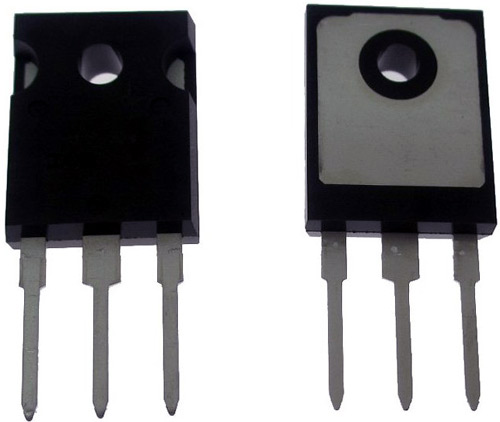
The IRFP150NPBF is another most common N-channel enhancement mode MOSFET designed with International Rectifier Fifth Generation Advanced HEXFET® Technology, to achieve extremely low on-resistance. It is used by many electronic designers because it comes in a TO-247 package, and it performs best with low voltage high current commercial-industrial applications.
Some basic features of IRFP150NPBF MOSFET are listed below:
- This MOSFET has a very low on-resistance of only 36 mΩ and a very low input capacitance of 2.8nF thus it can be used for high speed switching regulators.
- Dynamic dv/dt prevents false switching, oscillation or permanent damage of a MOSFET.
- This MOSFET is suitable for some of the industrial applications include high power SMPS circuit, constant current load and many more.
- Isolated Central Mounting Hole is a bonus.
Most Important Parameters
|
Rating |
Symbol |
Value |
Unit |
|
Drain−Source Voltage |
VDS |
100 |
Vdc |
|
Gate−Source Voltage − Continuous |
VGS |
± 20 |
Vdc |
|
Drain−Source On-Resistance (VGS = 10 Vdc,ID = 100 mAdc) |
RDS(on) |
0.055 |
Ω |
|
Drain Current - Continuous - Pulsed |
ID IDP |
41 160 |
Adc |
|
Total Device Dissipation @ TA = 25°C |
PD |
230 |
W |
|
Drain−Source Breakdown Voltage (VGS = 0, ID = 250 μA ) |
V(BR)DSS |
100 |
Vdc |
|
Total Gate Charge |
Qg (Max.) |
140 |
nC |
|
Gate Threshold Voltage (VDS = VGS, ID = - 250 μA) |
VGS(Th) |
4.0 |
Vdc |
|
Operating and Storage Junction Temperature Range |
TJ, Tstg |
- 55 to + 175 |
°C |
Part Number: IRFP150
Datasheet Link: Click here to open the datasheet
Similar Products: IRFP140NPBF, IRFP2907PBF, IRFP250MPBF, IRFP350PBF
Note: This is a common product and can be found in a local electronic parts store.
SiHG47N60E
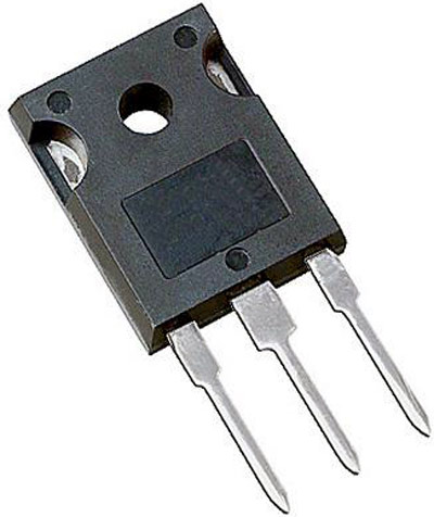
The SiHG47N60E is another most common N-channel enhancement MOSFET in the industry and it is designed by Vishay Siliconix. It comes in a TO-247AC package, so it is preferred for all commercial-industrial high voltage high current applications. Low thermal resistance and low package cost of the TO-247AC package make it very popular in the industry.
Some basic features and applications of SiHG47N60E are listed below:
- It has a drain to the source breakdown voltage of 650V and a constant load current of 32A which means it is used for very high power industrial applications.
- Low input capacitance of 9.62nF makes it perfect as a high voltage chopper driver.
- Although it is a very high power MOSFET, but it has a very low gate charge of only 220 nC which means it can be driven by a very cheap MOSFET gate driver IC.
- The Avalanche energy rating (UIS) makes it compatible with many applications.
- Some of the applications include
- Switch-mode power supplies (SMPS),
- Power factor correction power supplies
- Fluorescent ballast light
- High-intensity discharge lights
- Welding
- Induction heating
- Battery chargers
- Solar (PV inverters)
Most Important Parameters
|
Rating |
Symbol |
Value |
Unit |
|
Drain−Source Voltage |
VDS |
600 |
Vdc |
|
Gate−Source Voltage − Continuous |
VGS |
± 30 |
Vdc |
|
Drain−Source On-Resistance (VGS = 10 Vdc,ID = 24 Adc) |
RDS(on) |
.53 |
Ω |
|
Drain Current - Continuous - Pulsed |
ID IDP |
47 |
Adc |
|
Total Device Dissipation @ TA = 25°C |
PD |
357 |
W |
|
Drain−Source Breakdown Voltage (VGS = 0, ID = 250 μA ) |
V(BR)DSS |
600 |
Vdc |
|
Total Gate Charge |
Qg (Max.) |
220 |
nC |
|
Gate Threshold Voltage (VDS = VGS, ID = - 250 μA) |
VGS(Th) |
4 |
Vdc |
|
Operating and Storage Junction Temperature Range |
TJ, Tstg |
-55 to +150 |
°C |
Part Number: SiHG47N60E
Datasheet Link: Click here to open the datasheet
Similar Products: SIHG47N60E-GE3
Note: This is a common product and can be found in a local electronics parts store.
STB55NF06FP
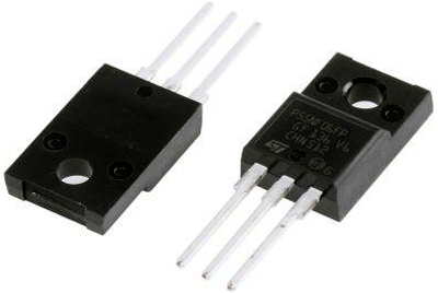
The STB55NF06FP is another most common N-channel enhancement type MOSFET designed by STMicroelectronics with its proprietary STripFET process. It comes in a TO-220FP package and can perform best with low voltage high current commercial-industrial applications, low thermal resistance. The low package cost of the TO-220FP makes it very popular in the industry.
Some basic features and applications of STB55NF06FP are listed below
- Low input capacitance of 1300pF makes it suitable for many high-speed switching applications.
- 7 V/ns dv/dt prevents false switching, oscillation or permanent damage of a MOSFET.
- This MOSFET has a very low gate charge of only 60 nC which means in a switching application. it can be driven by a very cheap MOSFET gate driver IC.
- Some of the applications include
- Switching Regulator
- DC-DC Converters
- Constant Current Load
Most Important Parameters
|
Rating |
Symbol |
Value |
Unit |
|
Drain−Source Voltage |
VDS |
60 |
Vdc |
|
Gate−Source Voltage − Continuous |
VGS |
± 20 |
Vdc |
|
Drain−Source On-Resistance (VGS = 10 Vdc,ID = 27.5 Adc) |
RDS(on) |
0.015 |
Ω |
|
Drain Current - Continuous - Pulsed |
ID IDP |
50 200 |
Adc |
|
Total Device Dissipation @ TA = 25°C |
PD |
30 |
W |
|
Drain−Source Breakdown Voltage (VGS = 0, ID = 250 μA ) |
V(BR)DSS |
60 |
Vdc |
|
Total Gate Charge |
Qg (Max.) |
60 |
nC |
|
Gate Threshold Voltage (VDS = VGS, ID = - 250 μA) |
VGS(Th) |
2 - 4 |
Vdc |
|
Operating and Storage Junction Temperature Range |
TJ, Tstg |
-55 to +150 |
°C |
Part Number: STB55NF06
Datasheet Link: Click here to open the datasheet
Similar Products: SiHG47N60E
Note: This is a common product and can be found in a local electronics parts store.
IPB035N08N3 G
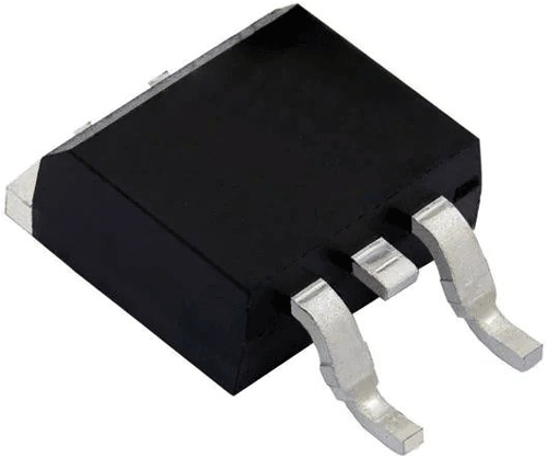
The IPB035N08N3 G is another unique N-channel enhancement MOSFET and it comes in a PG-TO263-3 package, so it has a fairly good thermal performance and performs best with low voltage high current applications. It is extremely low on-resistance of only 3.5mΩ which is another unique feature of this MOSFET and very low package cost of the PG-TO263-3 makes it a very cost-efficient solution for design and production purposes.
Some basic features and applications of IPB035N08N3 G are listed below:
- Ultra-low on-resistance of only 3.5mΩ and small size makes it a perfect choice for high-power dense electronic designs.
- Ideal for high-frequency switching applications due to low gate charge and low input capacitance.
- Low gate charge of only 30 nC and low on-resistance of 3.5mΩ product (FOM).
- The Avalanche energy rating (UIS) makes it compatible with many applications.
- Some of the applications include
- Switch-mode power supplies (SMPS),
- DC-DC converters
- Power Delivery System in a motherboard
- Constant current load
Most Important Parameters
|
Rating |
Symbol |
Value |
Unit |
|
Drain−Source Voltage |
VDS |
80 |
Vdc |
|
Gate−Source Voltage − Continuous |
VGS |
± 20 |
Vdc |
|
Drain−Source On-Resistance (VGS = 10 Vdc,ID = 100 Adc) |
RDS(on) |
0.0031 |
Ω |
|
Drain Current - Continuous - Pulsed |
ID IDP |
100 400 |
Adc |
|
Total Device Dissipation @ TA = 25°C |
PD |
214 |
W |
|
Drain−Source Breakdown Voltage (VGS = 0, ID = 21 mA ) |
V(BR)DSS |
80 |
Vdc |
|
Total Gate Charge |
Qg (Max.) |
117 |
nC |
|
Gate Threshold Voltage (VDS = VGS, ID = - 250 μA) |
VGS(Th) |
2 - 3.5 |
Vdc |
|
Operating and Storage Junction Temperature Range |
TJ, Tstg |
-55 to +175 |
°C |
Features:
- Ideal for high-frequency switching and sync. rec.
- Optimized technology for DC/DC converters
- Excellent gate charge x R DS(on) product (FOM)
- Very low on-resistance RDS(on)
- N-channel, normal level
- 100% avalanche tested
- Qualified according to JEDEC1) for target applications
- Halogen-free according to IEC61249-2-21
Applications: Solar, Telecom, Power distribution system e.g motherboard
Part Number: IPB035N08N3 G
Datasheet Link: Click here to open the datasheet
Similar Products: IPB048N15N5ATMA1, IPB025N10N3GATMA1, IPB014N06NATMA1, IPB011N04NGATMA1
Note: It is also not easily available in stores but can be bought online.


