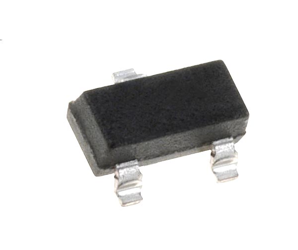
FDV301N N-Channel MOSFET
FDV301N is semiconductor device called MOSFET (Metal Oxide Semiconductor Field Effect Transistor) and is used as a high speed switching device in applications. The device is an N-Channel enhancement mode Field Effect Transistor that is produced using ON Semiconductor's proprietary, high cell density, DMOS technology. This very high density process is especially tailored to minimize ON state resistance. Also since the device is logic level MOSFET it can be triggered to ON by digital circuits voltage levels of +3.3V and+5V.
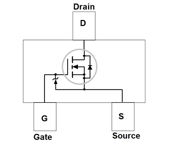
Pin configuration
FDV301N is a three pin device as shown in figure and the function of each of those pins is stated below.
|
Pin |
Name |
Function |
|
1 |
Drain |
Current comes in to the device from this pin. |
|
2 |
Gate |
MOSFET gets turned ON and OFF depending on voltage applied at this pin. |
|
3 |
Source |
Current which comes in to the device goes out through this pin. This pin is usually connected to ground. |
FDV301N Features and Electrical characteristics
- Logic level MOSFET - Very low level gate drive requirements allowing direct operation in 3V circuits.
- Very low turn ON resistance: RDS(ON) = 5Ω @ VGS= 2.7 V, RDS(ON) = 4Ω @ VGS= 4.5 V.
- Gate-Source Zener for ESD ruggedness(>6kV)
- Replace multiple NPN digital transistors with one DMOSFET.
- Maximum Drain-Source Voltage: 25V
- Maximum Gate-Source Voltage: 8V
- Maximum continuous Drain current: 0.22A
- Peak Drain current allowed: 0.5A
- Operating temperature range: -55ºC to 150ºC
- Maximum power dissipation: 0.35W
Similar MOSFETs
BF995, TP0101T, TP0202T, IRLML2402
FDV301N Uses
- FDV301N is a Digital MOSFET which can be trigger ON by applying voltages as low as 2.0V to its gate. With that being the case the device can be used in all low voltage digital circuits.
- FDV301N can also be as a high speed switching device replacing all conventional transistors in digital circuits since it is specifically designed for high speed switching applications.
- The device had very low turn ON resistance which is a must condition in some applications.
- The device is also preferred for high efficiency application as the low drop during switching leads to less power loss and with less power loss the efficiency of the system will be more.
How to use FDV301N
For understanding the working of FDV301N let us consider a simple application circuit as shown below.
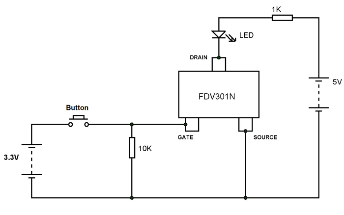
In the circuit FDV301N is used as a simple switching device with switching load being an LED. There are two power sources, one (5V) for powering the load LED and other (3.3V) for providing voltage to the gate of MOSFET. The button is the trigger to turn ON the device.
Now let us remember the characteristics of N-channel enhancement MOSFET:
- The MOSFET does not conduct when the voltage at the Gate-Source junction does not meet the threshold.
- The current flow through Drain is determined by the Gate voltage up to a certain point. So higher Gate voltage, lower the MOSFET conduction resistance and higher the drain current. Also the MOSFET conducts only during presence of Gate voltage so the instant the Gate voltage removed the MOSFET stops conducting.
The same characteristics will be applied to the device in the above circuit. So when the button is not pressed there will be no Gate voltage and the MOSFET will not conduct the current. With MOSFET acting as open circuit in the absence of Gate voltage the entire supply voltage of +5V appears across the device.
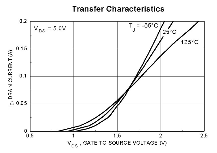
The instant the button is pressed a positive voltage of +3.3V appears at the gate of the device. And based on the transfer characteristics of the device shown in graph, a voltage of 2.5V at Gate is more than enough for the device to start conducting.
When the drain current flows a voltage appears across LED turning it ON and it will stay in that state till the button is released. With that we are switching the load ON and OFF by toggling the button. In high frequency application instead of button we will have microcontroller PWM or other control signal.
Hence by using the above circuit we have used FDV301N as a switching device and in a similar way we can use the device in other application circuits.
Applications
- DC-DC converters.
- Battery operated systems.
- Display drivers.
- Power management functions.
- Memory circuits.
- Basic switching applications.
- Relay drivers.
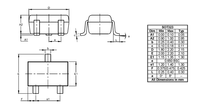
2D-Model