2N5089 NPN Amplifier Transistor
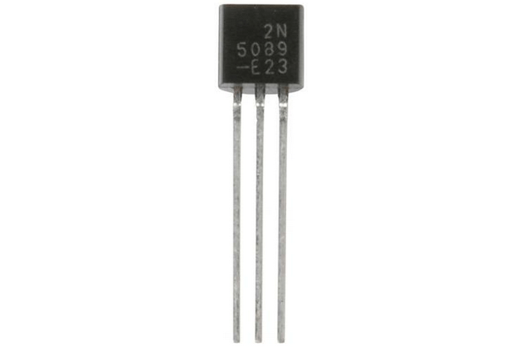
2N5089 is an NPN Silicon-based Amplifier Transistor that is widely used in audio equipment for amplification and other purposes. It has a Collector-Emitter Voltage of 25 Vdc with a Collector-Base voltage of 30 Vdc. The 2N5089 could provide 50mAdc of collector current continuously.
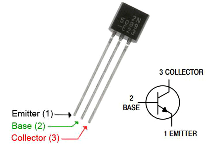
Pin Description of 2N5089 Transistor
|
Pin Number |
Pin Name |
Description |
|
1 |
Emitter |
Emitter pin of the transistor |
|
2 |
Base |
Base pin of the transistor |
|
3 |
Collector |
Collector pin of the transistor |
Features and Specification of 2N5089 Transistor
- Type: NPN
- Collector to Emitter Voltage (VCEO)= 25 Vdc
- Collector to Base Voltage (VCBO) = 30 Vdc
- Emitter to Base Voltage (VEBO)= 3.0 Vdc
- Collector Current (IC)= 50 mAdc
- Min hFE = 400 (when, IC = 100 Adc, VCE = 5.0 Vdc
- Max hFE = 1200 (when, IC = 100 Adc, VCE = 5.0 Vdc)
- Current-gain-bandwidth Product = 50 Mhz (IC = 500 Adc, VCE = 5.0 Vdc, f = 20 MHz)
- Small−Signal Current Gain = 450(min), 1800(max)
Note: Complete technical details can be found in the 2N5089 Datasheet, linked at the bottom of this page.
Alternative Product of 2N5089 Transistor
The exact equivalent for 2N5089 (SMD version) is MMBT5089 (SMD - SOT-23). Other Replacements for the 2N5089 transistor are MPS650, MPS6532, MPSH10, MPSW0, and ZTX690B.
2N5089 Transistor- Overview
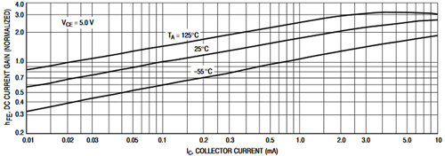
The 2N5089 is an NPN silicon transistor. It offers great hFE and is suitable for use in Audio amplification or specific audio-related products. The below graph is useful to know the characteristic of the transistor where the DC current gain is plotted against the Collector current.
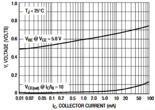
This transistor is also useful for switching related applications. The below graph is providing the “ON” voltages of the transistor against the collector current.
How to Choose a Transistor
1. Choose the transistor type that is required for the application. 2N5089 is an NPN transistor thus it is suitable to use on the low side of the power path. If the application requires high side switching, then use PNP.
2. Calculate the maximum Collector-Emitter voltage and the Collector-Base voltage will be for the targeted application. Choose a transistor that has the Collector-Emitter and Base-Emitter breakdown voltage more than what is actually required. 2N5089 supports 25V Collector-Emitter breakdown voltage and 30V Collector-Base Breakdown voltage.
3. Calculate maximum Collector Current. Choose a transistor that could tolerate more than the Collector current that is actually required for the application. 2N5089 works up to 50mA of continuous collector current (IC).
4. Choose the proper hFE (DC gain) and always check for the bandwidth for Audio related applications.
2N5089 - Interfacing Diagram
The below image is showing the standard application of the NPN transistor 2N5089 as an amplifier.
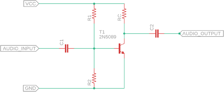
The C1 is the coupling capacitor and the C2 is the DC blocking capacitor where the output will be harvested. The RC is the collector Resistor and changing this value will change the frequency response of the circuit as well as it will control the DC gain by controlling the collector current. R1 and R2 are used as a voltage divider for biasing the transistor.
A typical value for 12V operation could be, R1 = 100k, R2 = 10k, RC = 10k, and C1, C2 can be 1uF ceramic capacitors.
Applications of 2N5089 Transistor
- Amplifier system
- Hi-Fi Audio system
- Push-pull topologies
- Tone control
- Switching applications
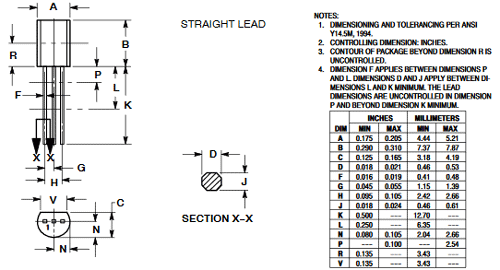
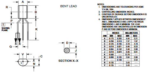
2D Model of 2N5089
The dimensions of 2N5089 in Straight Lead Package and Bent Lead Package are given below to help you with selecting the right PCB footprint for 2N5089.