GL850G - USB 2.0 hub controller
The GL850G is a highly regarded USB 2.0 hub controller manufactured by Genesys Logic, renowned for its exceptional performance and versatility. It supports up to 4 downstream ports, and also individual and gang mode for power management. Number of downstream ports and non/removable downstream port can be configured by different ways, such as EEPROM, SMBUS or I/O strapping. The upstream port supports both high speed and full speed specifications, while the downstream ports support high speed, full speed and low speed traffic. The GL850G is available in 48 pin LQFP, 28 pin SSOP and 24 pin QFN.
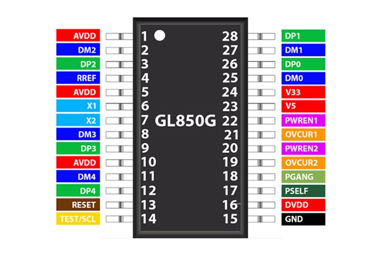
GL850G Pinout Configuration
|
Pin |
Name |
Function |
|
1 |
AVDD |
3.3V analog power input for analog circuits |
|
2 |
DM2 |
Downstream 2 port Data - |
|
3 |
DP2 |
Downstream 2 port Data + |
|
4 |
RREF |
Connect 680Ohms resistor between RREF and AGND |
|
5 |
AVDD |
3.3V analog power input for analog circuits |
|
6 |
X1 |
12MHz Oscillator input |
|
7 |
X2 |
12MHz Oscillator input |
|
8 |
DM3 |
Downstream 3 port Data - |
|
9 |
DP3 |
Downstream 3 port Data + |
|
10 |
AVDD |
3.3V analog power input for analog circuits |
|
11 |
DM4 |
Downstream 4 port Data - |
|
12 |
DP4 |
Downstream 4 port Data + |
|
13 |
RESET |
Active low external reset |
|
14 |
TEST/SCL |
Chip will be in test mode if pulled high/I2C Clock output |
|
15 |
GND |
Ground |
|
16 |
DVDD |
3.3V digital power input for digital circuits, Logic Level |
|
17 |
PSELF |
0: GL850G is bus powered 1:GL850G is self-powered |
|
18 |
PGANG |
Individual / Gang mode select |
|
19 |
OVCUR2 |
Active Low over current indicator |
|
20 |
PWREN2 |
Active Low power enable output |
|
21 |
OVCUR1 |
Active Low over current indicator |
|
22 |
PWREN1 |
Active Low power enable output |
|
23 |
V5 |
5V to 3.3V regulator input |
|
24 |
V33 |
3.3V regulator output |
|
25 |
DM0 |
Upstream port Data - |
|
26 |
DP0 |
Upstream port Data + |
|
27 |
DM1 |
Downstream 1 port Data - |
|
28 |
DP1 |
Downstream 1 port Data + |
Features
- Compliant to USB Specification Revision 2.0
- Upstream port supports both high-speed (HS) and full speed (FS) traffic
- Downstream ports support HS, FS, and low-speed (LS) traffic
- 1 control pipe (endpoint 0, 64-byte data payload) and 1 interrupt pipe (endpoint 1, 1-byte data payload)
- Backward compatible to USB specification Revision 1.1
- On-chip 8-bit micro-processor
- RISC-like architecture
- USB optimized instruction set.
- Performance: 6 MIPS @ 12MHz
- With 64-byte RAM and 4K mask ROM
- Support customized PID, VID by external EEPROM/ SMBUS/
- Support downstream port configuration by external EEPROM/ SMBUS/
- Single Transaction Translator (STT)
- Single TT shares the same TT control logics for all downstream port devices. This is the most cost-effective solution for TT.
- Integrate USB 2.0 transceiver.
- Improve output drivers with slew-rate control for EMI reduction.
- Internal power-fail detection for ESD recovery
- Low BOM cost
- Built-in 5V to 3.3V regulator
- Built-in upstream 1.5KΩ pull high and downstream 15KΩ pull-down.
- Built-in PLL supports external 12 MHz crystal / Oscillator clock input.
- Embed serial resister for USB signals.
- Low power support
- Support Selective Suspend
- Support LPM L1 with EEPROM
- Smart power mode
- Support both individual and gang modes of power management and over-current detection for downstream ports (Individual mode is not supported by SSOP 28 package)
- Conform to bus power requirements.
- Flexible design
- Number of Downstream port can be configured by SMBUS / EEPROM/
- Compound-device (non-removable in downstream ports) could be configured by I/O strapping/ SMBUS / EEPROM/
- Automatic switching between self-powered and bus-powered modes
- Available package:
- 28 pin QFN (5x5mm)
- 28 pin SSOP (209mil)
- 24 pin QFN (4x4mm
USB HUB Controllers Compatible with GL850G
GL852G
Other Popular USB HUB Controllers
FE1.1S, PL2586
Note: Complete technical details can be found in the GL850G datasheet at this page’s end.
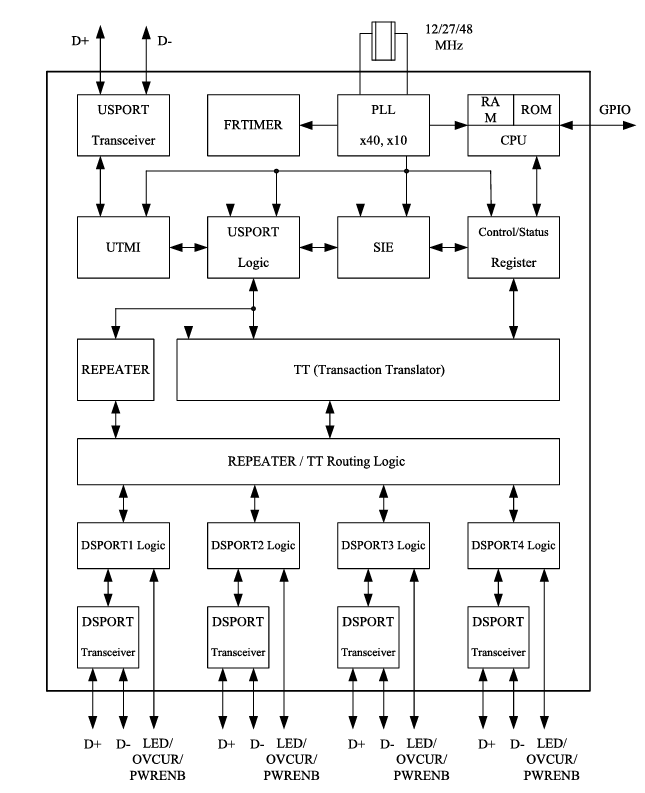
GL850G Block Diagram
GL850G Application Circuit Diagram
The following image shows the typical application circuit for the GL850G.
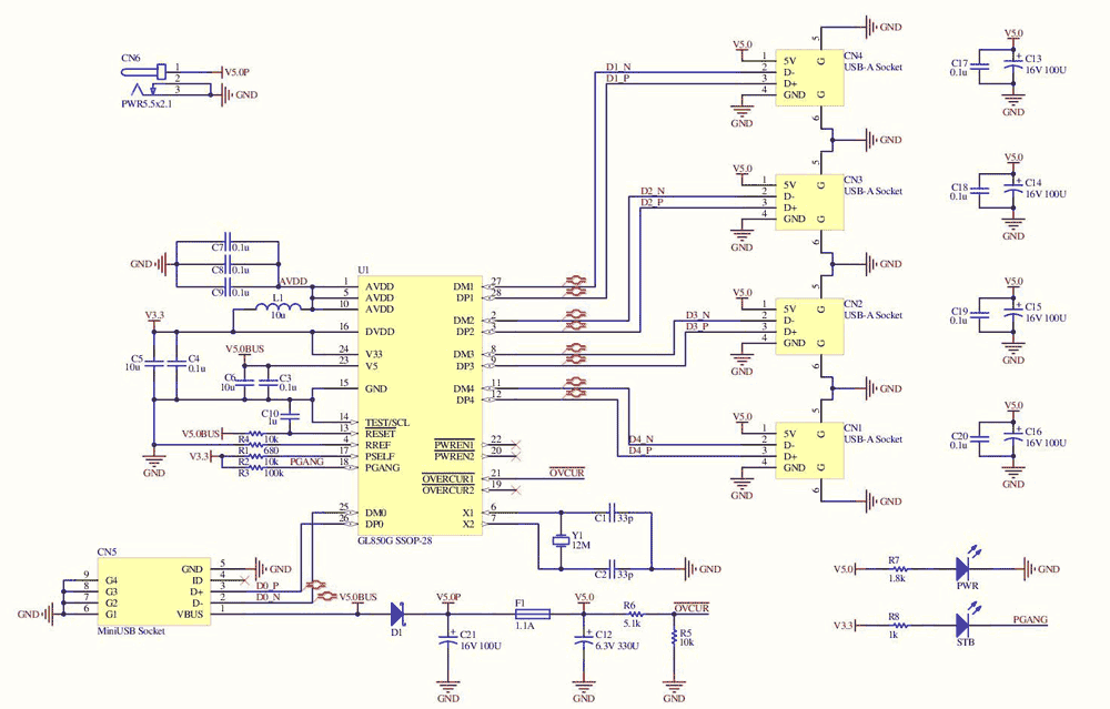
Apart from the crystal oscillator and USB ports, GL850G requires an output capacitor for filtering and stability purposes. Pullup resistors are used with the configuration pins.
Applications
- Standalone USB hub
- NB / Tablet / Motherboard / Docking Station
- Gaming console
- LCD monitor hub
- Any compound device to support USB hub function.
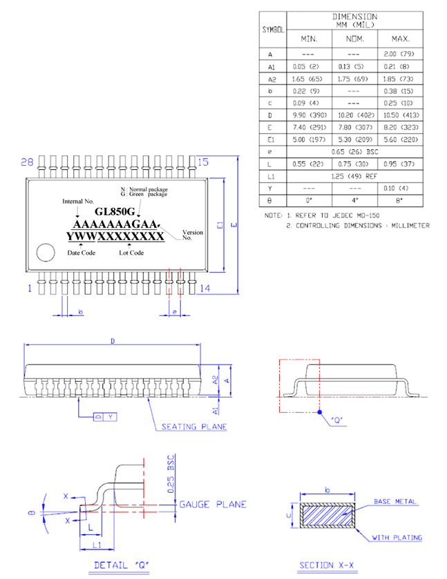
2D-Model and Dimensions
Below is the 2D CAD drawing of GL850G in SSOP28 package along with its dimensions in millimetres. The dimensions can be used to create custom footprints of the module and be used for PCB or CAD modelling. For other package dimensions please refer the datasheet at this page’s end.