CH32V003 - 32-bit General Purpose RISC-V MCU
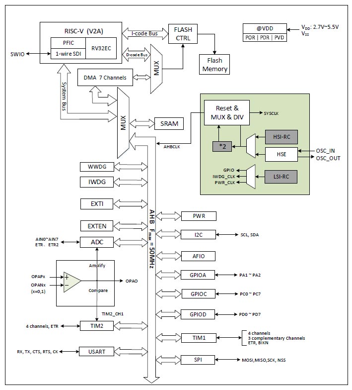
CH32V003 is a general purpose, industrial-standard microcontroller based on the QingKe RISC-V2A core's architecture. With a capability to reach clock frequency of 48MHz, the CH32V003 supports wide operating voltage, streamlined single-wire serial debugging approach, and low-power consumption. They are available in a variety of ultra small packages with a diverse set of peripheral functionalities. Among these are a dedicated DMA controller cluster, a 10-bit ADC unit, an op-amp comparator module, and an assortment of timers. To bolster its versatility, it also supports widely adopted communication platforms such as USART, I2C, and SPI. Its recommended operating voltages are either 3.3V or 5V, and it demonstrates resilience in industrial temperature conditions, ranging from -40℃ to 85℃
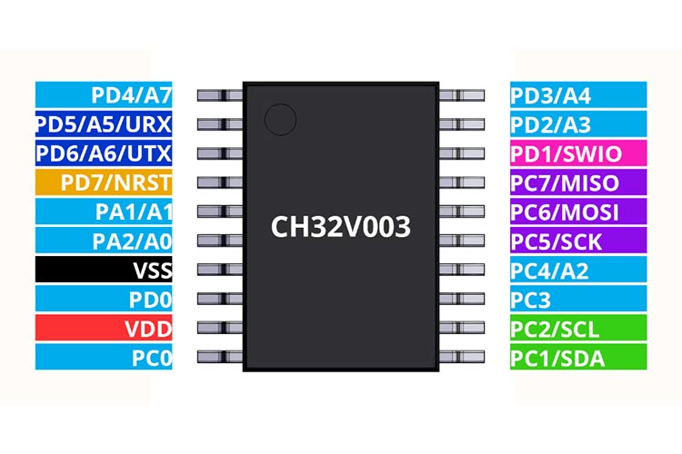
CH32V003 Pinout
|
Pin No |
Pin name |
Pin type |
Main function (after reset) |
Default alternate function |
Remapping function |
|||
|
SOP16 |
TSSOP20 |
QFN20 |
SOP8 |
|||||
|
|
- |
0 |
- |
VSS |
P |
VSS |
- |
- |
|
8 |
1 |
18 |
8 |
PD4 |
I/O/A |
PD4 |
UCK/T2CHIETR1/A7/ OPO |
TIETR_2/T1CH4_3 |
|
9 |
2 |
19 |
8 |
PD5 |
I/O/A |
PD5 |
UTX/A5 |
T2CH4_3/URX_2 |
|
10 |
3 |
20 |
1 |
PD6 |
I/O/A |
PD6 |
URX/A6 |
T2CH3_3/UTX_2 |
|
11 |
4 |
1 |
- |
PD7 |
I/O/A |
PD7 |
NRST/T2CH4/OPP1 |
UCK_1/UCK_2/T2CH4_2 |
|
12 |
5 |
2 |
1 |
PA1 |
I/O/A |
PA1 |
TICH2/A1/OPN0 |
OSCI/TICH2_2 |
|
13 |
6 |
3 |
3 |
PA2 |
I/O/A |
PA2 |
TICH2N/A0/OPPO |
OSCO/AETR2_1/TICH2N_2 |
|
14 |
7 |
4 |
2 |
VSS |
P |
VSS |
- |
- |
|
- |
8 |
5 |
- |
PD0 |
I/O/A |
PD0 |
TICHIN/OPN1 |
SDA_1/UTX_1/TICHIN_2 |
|
15 |
9 |
6 |
4 |
VDD |
P |
VDD |
- |
|
|
16 |
10 |
7 |
- |
PC0 |
I/O |
PC0 |
T2CH3 |
NSS_1/UTX_3/T2CH3_2 /T1CH3_1 |
|
1 |
11 |
8 |
5 |
PC1 |
I/O/FT |
PC1 |
SDA/NSS |
T1BKIN_1/T2CH4_1 T2CH1ETR(2)2URX_3 /T2CH1ETR1)_3/T1BKIN_3 |
|
2 |
12 |
9 |
6 |
PC2 |
I/O/FT |
PC2 |
SCL/URTS/T1BKIN |
AETR_1/T2CH2_1 /T1ETR_3/URTS_1 /T1BKIN_2 |
|
3 |
13 |
10 |
- |
PC3 |
I/O |
PC3 |
TICH3 |
T1CH1N_1/UCTS_1 /T1CH3_2/T1CH1N_3 |
|
4 |
14 |
11 |
7 |
PC4 |
I/O/A |
PC4 |
T1CH4/MCO/A2 |
T1CH2N_1/T1CH4_2 /TICH1_3 |
|
- |
15 |
12 |
- |
PC5 |
I/O/FT |
PC5 |
SCK/T1ETR |
/SCL_3/UCK_3/T1ETR_1 /T1CH3_3/SCK_1 |
|
5 |
16 |
13 |
- |
PC6 |
I/O/FT |
PC6 |
MOSI |
T1CH1_1/UCTS_2/SDA_2 /SDA_3/UCTS_3/T1CH3N_ 3 /MOSI_1 |
|
6 |
17 |
14 |
- |
PC7 |
I/O |
PC7 |
MISO |
TICH2_1/URTS_2 /T2CH2_3/URTS_3 /T1CH2_3/MISO_1 |
|
7 |
18 |
15 |
8 |
PD1 |
I/O/A |
PD1 |
SWIO/T1CH3N/AETR2 |
SCL_1/URX_1/T1CH3N_1 /T1CH3N_2 |
|
- |
19 |
16 |
- |
PD2 |
I/O/A |
PD2 |
TICH1/A3 |
T2CH3_1/T1CH2N_3 /T1CH1_2 |
|
- |
20 |
17 |
- |
PD3 |
I/O/A |
PD3 |
A4/T2CH2/AETR/UCTS |
T2CH2_2/T1CH4_1 |
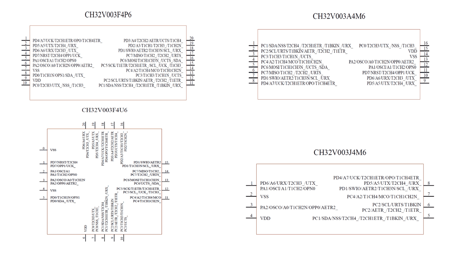
CH32V003 Other available packages
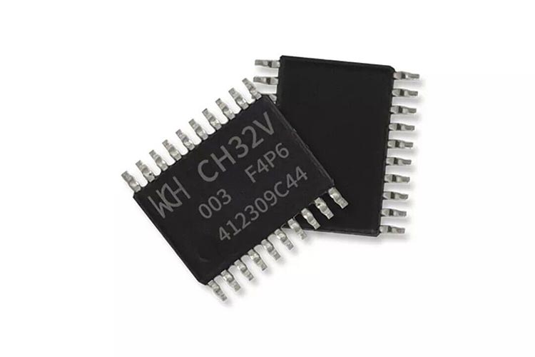
CH32V003F4P6, CH32V003A4M6, CH32V003F4U6, CH32V003J4M6
Features
- Core
- QingKe 32-bit RISC-V core, RV32EC instruction set.
- Fast programmable interrupt controller + hardware interrupt stack
- Support 2-level interrupt nesting
- Support system main frequency 48MHz
- Memory
- 2KB volatile data storage area SRAM
- 16KB program memory CodeFlash
- 1920B BootLoader
- 64B non-volatile system configuration memory
- 64B user-defined memory
- Power management and low-power consumption
- System power supply VDD: 3.3V or 5V
- Low-power mode: Sleep, Standby
- Clock & Reset
- Built-in factory-trimmed 24MHz RC oscillator
- Built-in 128KHz RC oscillator
- High-speed external 4~25MHz oscillator
- Power on/down reset, programmable voltage detector
- 1 group of 1-channel general-purpose DMA controller
- 7 channels, support ring buffer
- Support TIMx/ADC /USART/I2C/SPI
- 1 group of OPA and comparator: connected with ADC and TIM2 1 group of 10-bit ADC
- Analog input range: 0~VDD
- 8 external signals + 2 internal signals
- Support external delayed triggering.
- Multiple timers
- 1 16-bit advanced-control timers, with dead zone control and emergency brake; can offer PWM complementary output for motor control.
- 1 16-bit general-purpose timers, provide input capture/output comparison/PWM/pulse counting/incremental encoder input.
- 2 watchdog timers (independent watchdog and window watchdog)
- SysTick: 32-bit counter
- Communication interfaces
- 1 USART interfaces
- 1 I2C interfaces
- 1 SPI interfaces
- GPIO port
- 3 groups of GPIO ports, 18 I/O ports
- Mapping 1 external interrupt
- Security features: 64-bit unique ID
- Debug mode: 1-wire serial debug interface (SDI)
- Package: SOP, TSSOP or QFN
CH32V003 Internal Block Diagram
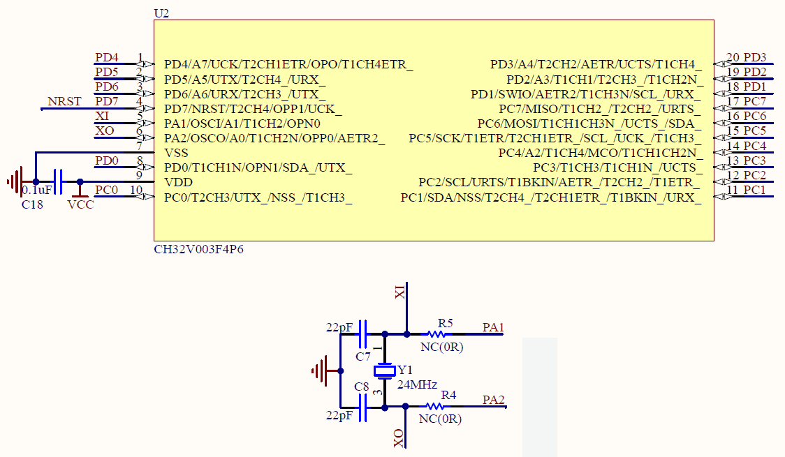
How To Use CH32V003?
This is the typical application circuit of the CH32V003 MCU with bare minimum components. As you can see there are only bare minimum components. Even the External crystal circuit is also optional. CH32V003 can be used with the internal RC clock.
Applications
- Low-cost consumer devices
- USB gamepads
- USB controllers
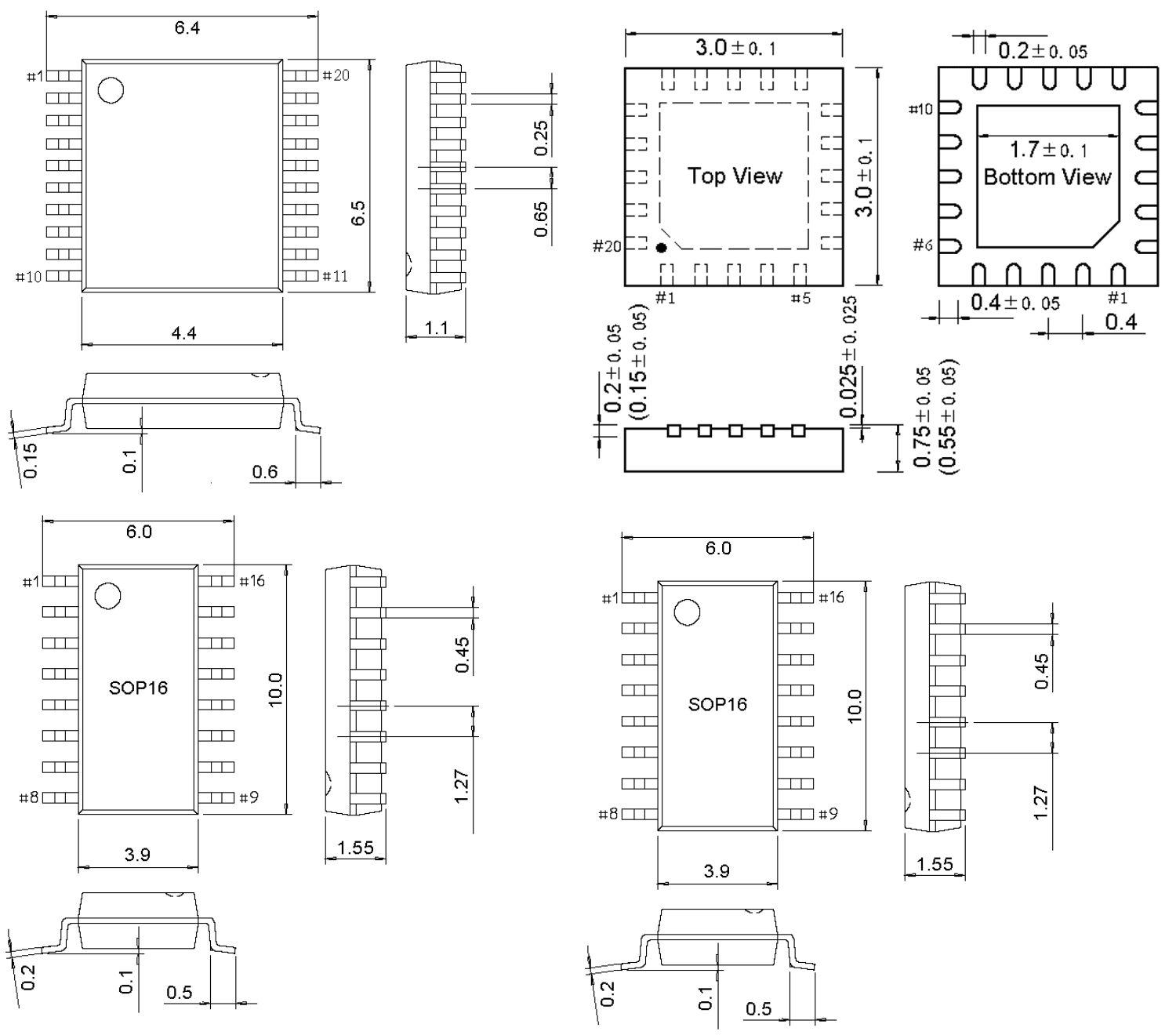
2D-Model and Dimensions