ADS1015 Low-Power, 12-Bit Analog-to-Digital Converter with Internal Reference
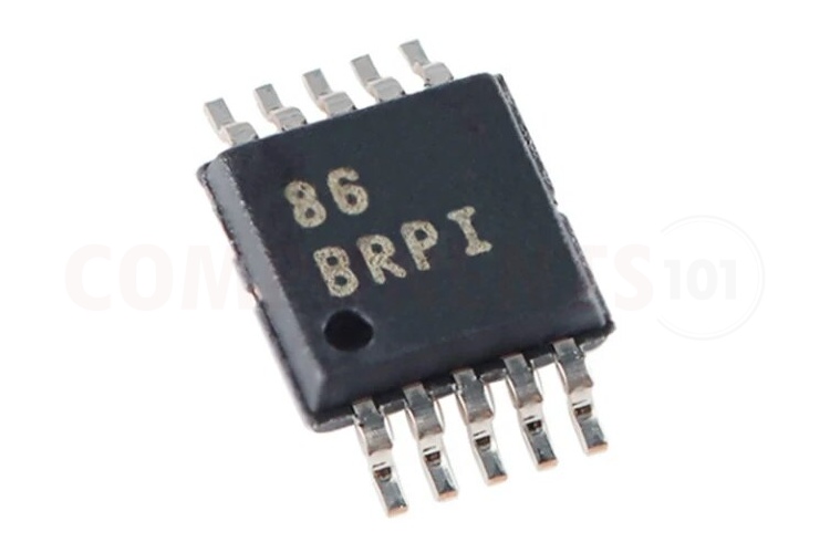
The ADS1015 is a high precision, low-power, 12-bit, I2C compatible, analog-to-digital converter (ADC). The ADS1015 includes a low-drift voltage reference and an oscillator. The internal voltage reference provides a stable reference voltage for the analog-to-digital converter (ADC), while the oscillator generates the clock signal needed for the ADC's operation. It also includes a programmable gain amplifier (PGA) and a digital comparator. The PGA allows you to adjust the gain of the ADC to amplify small analog signals for better resolution. The digital comparator can be used to compare the converted analog signal with a programmable threshold value. These additional features make the ADS1015 a versatile device for precision analogue-to-digital conversion in various sensor and measurement applications. Wide operating supply range, makes the ADS1015 well-suited for power and space-constrained, sensor measurement applications. The ADS101x perform conversions at data rates up to 3300 samples per second (SPS). The ADS1015 features an input multiplexer (MUX) that allows two differential or four single-ended input measurements. The device is automatically powered down after one conversion in single-shot mode; therefore, power consumption is significantly low. The ADS1015 is available in a very small X2QFN-10 package and a VSSOP-10 package.
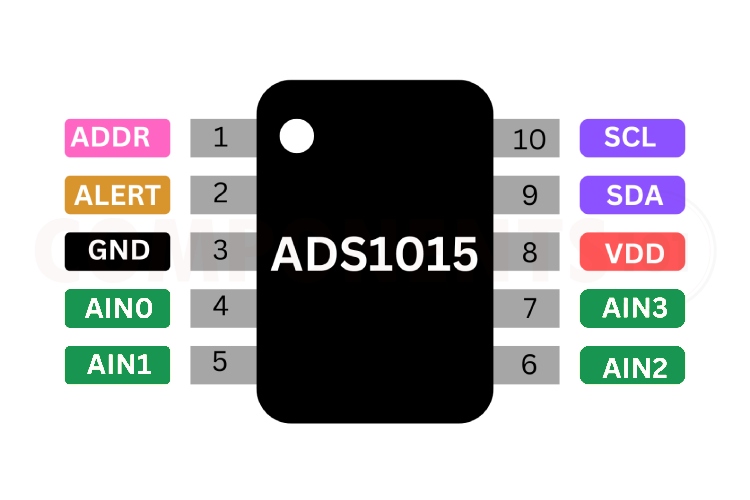
ADS1015 Pinout Configuration
Here are the pinout details for ADS1015.
| PIN NO | PIN NAME | DESCRIPTION |
| 1 | ADDR | I2C slave address select |
| 2 | ALERT//RDY | Alert output |
| 3 | GND | Ground |
| 4 | AIN0 | Analog input |
| 5 | AIN1 | Analog input |
| 6 | AIN2 | Analog input |
| 7 | AIN3 | Analog input |
| 8 | VDD | Power supply |
| 9 | SDA | Serial data |
| 10 | SCL | Serial clock input |
ADS1015 Features
ADS1015 ADC has the following key features:
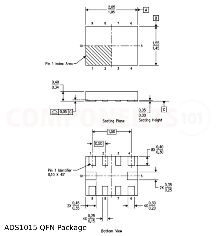
- Ultra-Small X2QFN Package: 2 mm × 1.5 mm × 0.4 mm
- 12-Bit Noise-Free Resolution
- Wide Supply Range: 2.0 V to 5.5 V
- Low Current Consumption: 150 μA (Continuous-Conversion Mode)
- Programmable Data Rate: 128 SPS to 3.3 kSPS
- Single-Cycle Settling
- Internal Low-Drift Voltage Reference
- Internal Oscillator
- I2C Interface: Four Pin-Selectable Addresses
- Four Single-Ended or Two Differential Inputs
- Programmable Comparator
- Operating Temperature Range: –40°C to +125°C
Manufacturers of ADS1015:
The ADS1015 is manufactured by Texas Instruments. There are no alternative manufacturers for the same part number as of the date of writing this article.
ADS1015 Equivalents
If you are looking for an equivalent or replacement for ADS1015, you can use ADS1013 and ADS1014
ADS1015 Alternatives
If you are looking for an alternative for ADS1015 you can look at the other IC from these.
AD7791, HX711, MCP3008, ADS1115, ADC0804, MCP3301, ADC0831.
Note: Complete technical details can be found in the ADS1015 datasheet at this page’s end.
ADS1015 Schematics
The following image shows the ADS1015 application circuit diagram.
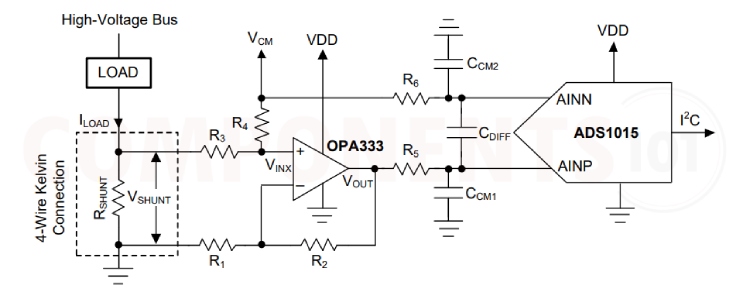
Shunt-based, current-measurement solutions are widely used to monitor load currents. Low-side, current-shunt measurements are independent of the bus voltage because the shunt common-mode voltage is near the ground. The above image shows an example circuit for a bidirectional, low-side, current-shunt measurement system. The load current is determined by measuring the voltage across the shunt resistor that is amplified and level-shifted by a low-drift operational amplifier, OPA333. The OPA333 output voltage is digitized with ADS1015 and sent to the microcontroller using the I2C interface. This circuit is capable of measuring bidirectional currents flowing through the shunt resistor with great accuracy and precision.
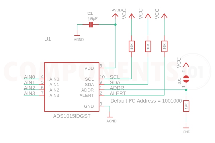
Here is a simplified circuit diagram of ADS1015. You can follow this for Arduino ADS1015 interfacing.
Troubleshooting Tips for ADS1015
- The circuit’s performance is not stable. There is a lot of noise introduced to the line: Ensure that the power supply to the ADS1015 is stable and within the specified voltage range. Connect a .1uf capacitor in between the supply voltage pin and the ground.
- I2C communication is not working: First check the hardware connections. Make sure that the SDA and SCL pins are connected to the I2C pins of the microcontroller. Use the I2C scanner program to find the device and address.
- Not getting any signals from the IC: Make sure that the ADS1015 is powered correctly according to the specified voltage levels and current requirements. Double-check all the connections, including I2C lines, reference voltage inputs, and analog input signals, to ensure they are properly connected. Should use pull-up resistors on the I2C lines.
Design Tips for ADS1015:
1. How to minimize noise while using LTC2400?
Good decoupling is important when using high-resolution ADCs. Vcc should be decoupled with .1 µF capacitors to GND. To achieve the best from these decoupling components, they should be placed as close as possible to the device, ideally right up against the device.
2. Is it possible to use it without microcontroller?
Since ADS1015 uses I2C communication we can't use the IC without a microcontroller.
3. What are the design considerations while designing PCBs using ADS1015?
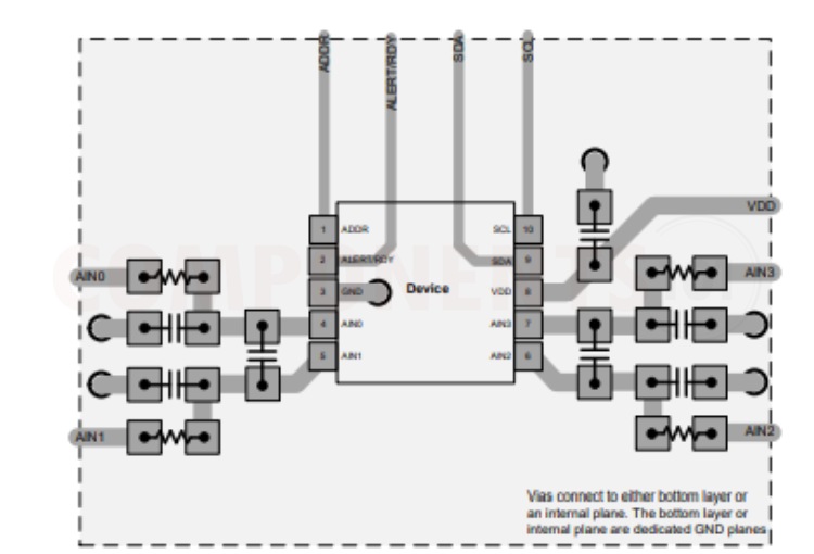
An example of good component placement is shown in the above image. Although it provides a good example of component placement, the best placement for each application is unique to the geometries, components, and PCB fabrication capabilities employed. That is, there is no single layout that is perfect for every design and careful consideration must always be used when designing with any analog component.
The following outlines some basic recommendations for the layout of the ADS101x to get the best possible performance of the ADC. A good design can be ruined with a bad circuit layout.
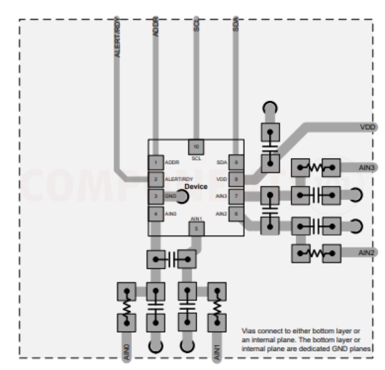
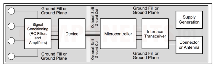
- Separate analog and digital signals. To start, partition the board into analog and digital sections where the layout permits. Route digital lines away from analog lines. This prevents digital noise from coupling back into analog signals.
- Fill void areas on signal layers with ground fill.
- Provide good ground return paths. Signal return currents flow on the path of least impedance. If the ground plane is cut or has other traces that block the current from flowing right next to the signal trace, it has to find another path to return to the source and complete the circuit. If it is forced into a larger path, it increases the chance that the signal radiates. Sensitive signals are more susceptible to EMI interference.
- Use bypass capacitors on supplies to reduce high-frequency noise. Do not place vias between bypass capacitors and the active device. Placing the bypass capacitors on the same layer as close to the active device yields the best results.
- Consider the resistance and inductance of the routing. Often, traces for the inputs have resistances that react with the input bias current and cause an added error voltage. Reduce the loop area enclosed by the source signal and the return current in order to reduce the inductance in the path. Reduce the inductance to reduce the EMI pickup and reduce the high-frequency impedance seen by the device.
- Differential inputs must be matched for both the inputs going to the measurement source.
- Analog inputs with differential connections must have a capacitor placed differentially across the inputs. Best input combinations for differential measurements use adjacent analog input lines such as AIN0, AIN1 and AIN2, AIN3. The differential capacitors must be of high quality. The best ceramic chip capacitors are C0G (NPO), which have stable properties and low-noise characteristics.
Applications of ADS1015
- Portable Instrumentation
- Battery Voltage and Current Monitoring
- Temperature Measurement Systems
- Consumer Electronics
- Factory Automation and Process Control
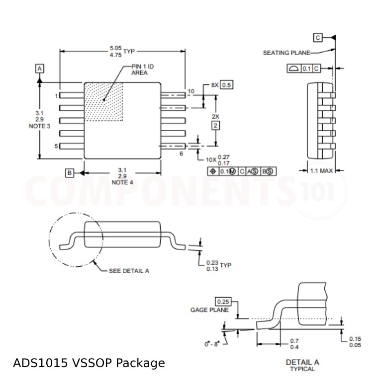
ADS1015 Package Options
The ADS1015 is available in two different packages VSSOP and X2QFN. The VSSOP package chips are available in the following part numbers: ADS1015IDGSR, ADS1015IDGST and the X2QFN packaged chips are available in the following part numbers: ADS1015IRUGR, ADS1015IRUGT. Other than the different chip packages all these are the same. The only difference between these two types is the number of chips per ordering package. The part numbers given above are currently active and can be used as drop-in replacements for obsolete part numbers such as ADS1015AQDGSRQ1 or ADS1015BQDGSRQ1.
You can also get ADS1015 modules for testing purposes. They can be directly connected with development boards such as Arduino.
2D Model and Dimensions of ADS1015
Here you can find the mechanical drawings of ADS1015 along with its dimensions. The dimensions can be used to create custom footprints of the module and be used for PCB or CAD modelling.