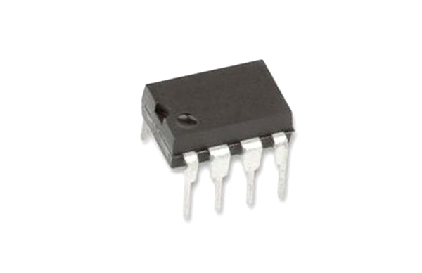
6N139 - High Gain Optocoupler IC
6N139 is an optocoupler IC designed for isolating primary circuit and secondary circuit electrically but the pair of LED and photodiode - Darlington setup forms the triggering mechanism between the two sides. The chip designed for Low input current, high gain, and High speed switching applications.
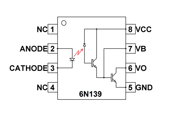
6N139 Pin Configuration
6N139 is an eight pin device and function of each pin is stated below. The device is available in various packages for choosing.
|
Pin Number |
Pin Name |
Description |
|
1 |
NC |
No connection |
|
2 |
Anode |
Positive terminal of internal LED |
|
3 |
Cathode |
Negative terminal of internal LED |
|
4 |
NC |
No connection |
|
5 |
GND |
Emitter of internal Darlington transistor which is connected to ground pin in circuit |
|
6 |
VO |
Collector of second transistor Darlington setup which is usually connected to load to receive current |
|
7 |
VB |
Base of second transistor Darlington setup |
|
8 |
VCC |
Collector of first transistor Darlington setup which is connected to positive power supply |
6N139 Features and Specifications
- CMOS, LSTTL compatibility
- High current transfer ratio
- Additional base pin access allows gain bandwidth adjustment
- Low input current requirements – 0.5 mA
- High output current
- Interfaces with common logic families
- High common mode rejection, 500 V/μs
- Performance guaranteed over temperature range: 0°Cto 70°C
- IR LED forward voltage for turning ON (VF): 1.4V
- Maximum IR LED forward voltage: 1.7V
- Maximum IR LED forward current during ON (IF): 25mA
- Maximum IR LED reverse voltage: 5V
- Maximum IR LED reverse current: 10uA
- Maximum supply and output voltage (Pin 8 to 5, pin 6 to 5): 18V
- Maximum current allowed trough transistor collector(IC): 60mA
- Current transfer ration (CTR): 400%
- Typical Rise Time: 1.5µs
- Typical Fall Time: 0.6µs
- Maximum output power dissipation: 100mW
6N139 Equivalents
6N138, HCPL-0701, HCPL-0700, HCNW139, HCNW-138
6N139 Optocoupler Overview
6N139 IC is basically used when you want to isolate two circuits electrically but still want to have a direct control mechanism. The device applications are many and a few main are stated below
- 6N139 can be used in applications where control unit can only provide low current signals. This is because of Darlington pair the gain of output is very high leading to the device being capable of driving at very low input current.
- 6N139 can be used in applications where switching frequency is high because the device being specifically designed to be installed in high frequency switching applications.
How to use 6N139 Optocoupler
As described in 6N139 pin diagram, the chip has three main components. And they are IR LED, Photo Diode and Darlington transistor setup. For understanding the working we will connect chip with other few components to form an example circuit.
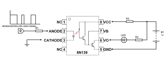
In circuit:
- The chip gets trigger pulses (or logic signal) from microcontroller and these voltage pulses are fed to IR LED in the IC as shown in above circuit. This setup act as INPUT or control circuit.
- The Darlington transistor is powered from a second power source of 12V and resistor R3 is for limiting the current flow when transistor starts conducting.
- The output response for given input is seen at ‘VO’ pin and here an LED is connected to visualize that response. And here resistor R2 is connected to limit the current through LED.
At a given time we will get +3.3V logic pulses from the microcontroller as shown in above diagram and they act as INPUT. Once these voltage pulses reach IR LED it will emit Infrared rays internally and these rays will fall on the photodiode. Based on the characteristic of photodiode upon receiving this radiation the device will start conducting in reverse bias direction in the presence of reverse voltage. As can be seen in internal structure once photodiode starts conducting the base of first transistor receives current and thereby it starts conducting. The current from first transistor drives the second transistor in to conduction as the emitter of first transistor is connected to base of second transistor.
When this transistor gets turned ON the current will be allowed to flows through its collector and with this flow a voltage appears across the load led turning it ON. Thus the led will light up when microcontroller provides HIGH logic to the chip at the input.
Once the microcontroller signal goes LOW the led at the output also gets turned OFF. By this control of primary circuit on secondary circuit via light triggering we have achieved the electrical isolation using device 6N139. In a similar way we can use 6N139 in other circuit applications.
Applications
- Digital logic ground isolation
- Telephone ring detector
- Lighting systems
- PWM applications
- AC mains detection
- Reed relay driving
- Switch mode power supply feedback
- Telephone ring detection
- High common mode noise line receiver
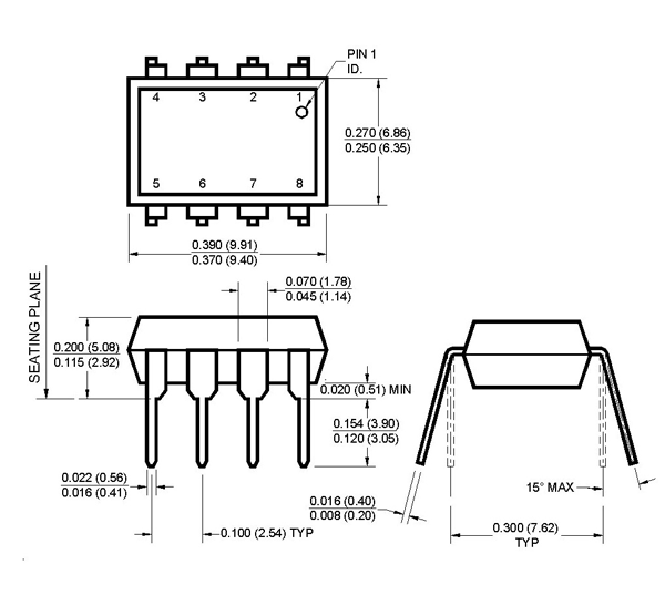
2D-Model
All measurements are in inches and measurements in brackets are scaled in millimeter