

Capable of supporting up to 32 GT/s without altering design
An Overview of MESFET Construction, Applications and Types

The average person who dabbles in electronics might be familiar with BJTs (Bipolar Junction Transistor) and MOSFETs (Metal Oxide Semiconductor Field Effect Transistor), some more experienced people might know about JFETs (Junction Field-Effect Transistor) and maybe even IGBTs – but these are not all the types of transistors that exist. Apart from these devices there exists a plethora of more exotic types, such as heterojunction bipolar transistors, dual gate MOSFETs, unijunction transistors, high electron-mobility transistors and Metal–Semiconductor Field-Effect Transistors, about which we will talk about in this article. They are similar in behaviour and construction to a JFET, having a reverse-biased junction that changes the width of a depletion zone, controlling drain current.
Applications of MESFET
The GaAs MESFET is a type of a metal–semiconductor field-effect transistor typically used at extremely high frequencies up to 40GHz in both high power (below 40W, above that TWT valves take over) and low power applications, such as:
- Satellite communications
- Radar
- Cell Phones
- Microwave communication links
They are used there, due to its excellent performance at higher frequencies, low noise and high gain.
Types of MESFET
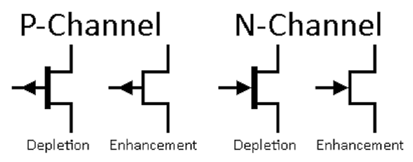
MESFET exists in P-channel and N-channel types, but mostly N-channel are used, because the electron mobility is around 20 times the hole mobility for GaAs and in N-channel electrons are the main charge carriers, not holes like in P-channel types.
Apart from channel type they can be divided into depletion and enhancement modes – in depletion at zero gate bias, drain current flows and at max. bias (cutoff) the current is zero. In enhancement the transistor is normally allowing drain current to flow and only after applying appropriate bias, drain current flows. Most MESFETs are N-channel depletion mode.
MESFET Operation and Construction
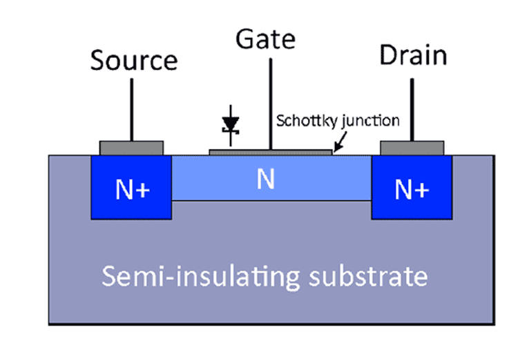
The transistor consists of a layer of lightly n-doped semiconductor (usually GaAs), called a channel, etched into a semi-insulating substrate, with an area of heavily n-doped semiconductor on each end, called either the source or the drain. The top side of the channel is coated with metal, forming a Schottky junction. This electrode, called the gate, if negatively biased (positive for P-Channel types) can control the flow of current through the channel, by establishing a charge carrier-devoid depletion region near the gate metallisation, in turn limiting the channel current. This is known as carrier channel width modulation, the process being comparable to clamping a water hose, reducing water flow.
In depletion mode MESFETs- by making the gate more negative the depletion channel is enlarged, because negative electrons are repelled by the negative gate voltage, in P-channel devices making the gate voltage more positive achieves this. In enhancement mode devices- the depletion zone normally covers the whole channel at Vg=Vs and no drain current flows, only when a positive (for N-channel types) is applied the depletion channel reduces, allowing for current flow.
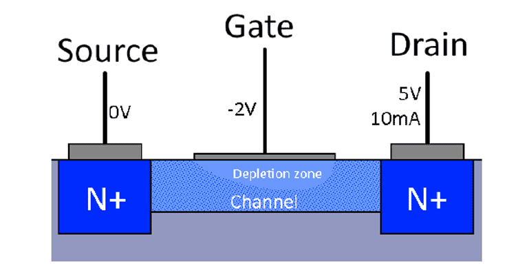
The depletion zone, notice it being shifted towards the positive drain.
In real life MESFET circuits the device should be biased so at no point during operation the gate voltage allows for the gate-channel diode to conduct, for N-channel GaAs devices the gate-source voltage can’t rise above 0.1-0.3V as this would cause current to flow through the delicate gate, destroying it. MESFETs are easily damaged by static discharges.
Advantages of GaAs MESFETs over other Transistors
- Better SHF and UHF performance
- High input impedance
- Very low noise figure
- Low parasitic capacitances
The better high frequency performance is allowed by the very high electron mobility of GaAs, it being over five times that of silicon (8500 cm2 V-1s-1 vs 1400 cm2 V-1s-1). The high input impedance is typical of all FETs. The very low noise figure is caused by the buried channel and the charge carries not going through surface states. The low parasitic capacitance is due to the Schottky type gate-channel junction, in a JFET this junction is of a p-n type, having higher capacitances.
Their main disadvantage is their high cost, due to GaAs being much harder than silicon and a high number of devices failing to work after being made.


